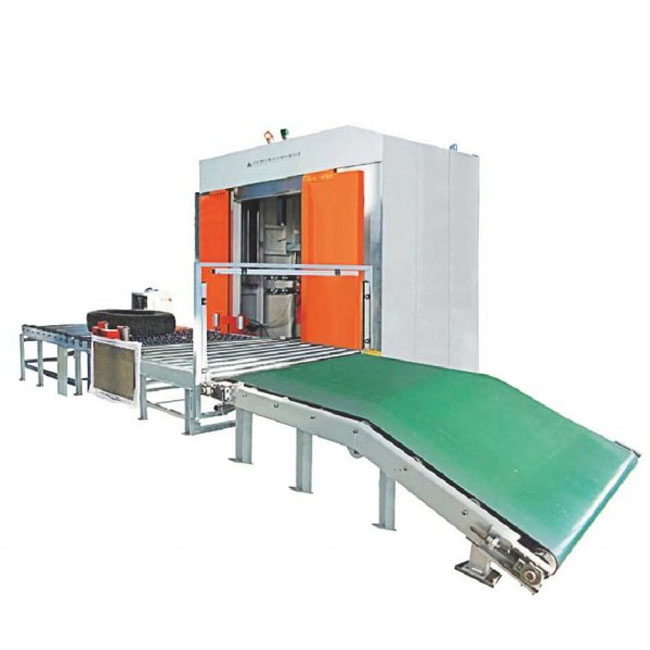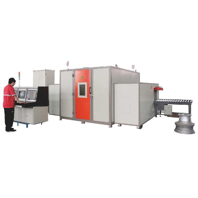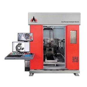
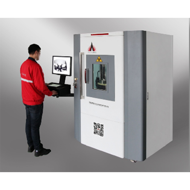
Digital Micro Focus X-ray Pcb Inspection System

- Aolong
- China
- 15 days
- 80pc/year
1. The pcb inspection system is applied to BGA/CSP and flip chip, Welds of PCB, Various battery, lC encapsulation, Capacitance and resistance, lnner defect of the metal material and dielectric material, etc.
2. The x-ray inspection system is a high-tech product which integrates with modern computer software technology, precision mechanical technology, optical technology, electronic technology.
Applications of Digital Micro Focus x-ray pcb inspection system
● Digital Micro Focus X-ray inspection system of BGA, CSP and flip chip
● Welds of PCB inspection system
● Digital Micro Focus X-ray inspection system of various battery
● lC encapsulation
● Capacitance and resistance
● lnner defect of the metal material and dielectric material
● lnner structure and module of the light weight material
● Electrothermal pipe, pearl and precision Components
What is an X-ray PCB inspection system?
Aolong's Digital Micro Focus X-ray PCB inspection system is a high-end nondestructive testing device specifically designed for inspecting printed circuit boards (PCBs) and electronic components. The X-ray PCB inspection system utilizes a high-brightness, micro-focus X-ray source to penetrate the circuit board material. High-resolution digital detectors produce clear images, allowing for intuitive visualization of solder joints, BGA packages, microcircuits, and the detailed internal structures of multilayer boards.


PCB Inspection System's Automatic Defect Detection Function:
Our Digital Micro Focus X-ray inspection system's automatic defect detection function accurately detects common defects such as pores, cracks, inclusions, and shrinkage. Using intelligent algorithms, it provides real-time alerts and data traceability, significantly reducing the cost and error of manual inspections. In customers' foundries or welding lines, the Digital Micro Focus X-ray PCB Inspection System automatically scans and identifies potential defects immediately after product forming or welding, preventing unqualified products from entering subsequent processes and improving production efficiency.
Key Features of the Image Processing System for the Micro focus PCB inspection system:
Micro focus PCB inspection system enables virtual 3D imaging and real-time image zooming and reduction
Grayscale optimization, real-time simulation, and user-friendly design
Electronic capture and multi-frame overlay for quick and convenient operation
Supports front and back imaging and edge strength
Precise curve measurement and statistics
BGA solder joint measurement technology
Measures angle, radius, solder ball area, and porosity
Calculates porosity ratio and solder ball coordinate statistics
Multiple output methods including dynamic storage, printing, and DVD read/write

Main Parameters of Micro focus PCB inspection system
| Tube voltage range | 20kV~160kV |
| Tube current range | 0.1μA~1000μA |
| JIMA Resolution | 0.5μm~2μm |
| Magnification | 20 times~3000 times |
| Micro focus PCB inspection system | |
| The inspect platform can move along x,y and z axes | |
The X-ray PCB Inspection System's In-Line Inspection Capabilities:
On a customer's electronic component production line, the Micro focus PCB inspection system can be integrated into the manufacturing process to monitor the internal density and defects of each cell in real time. This immediate feedback allows the production team to quickly adjust process parameters and reduce the risk of mass scrap. Our X-ray Inspection System significantly improves the efficiency of our customers' production lines and increases production capacity. Many of our customers have experienced significant increases in production efficiency after using our X-ray Inspection System, making it a perfect fit for companies involved in electronic components.

Our After-Sales Support:
Aolong offers a comprehensive service and support program for our X-ray inspection systems. Our team of experts provides comprehensive pre-training to help operators familiarize themselves with system functions and maximize efficiency from the outset. If any equipment issues arise, we have a response mechanism and rapid repair solutions to restore your equipment to normal operation as quickly as possible, minimizing losses caused by unplanned downtime.

FAQs of x-ray pcb inspection system:
1. What defects can x-ray pcb inspection system primarily detect?
X-ray inspection system can accurately detect common hidden defects such as cold solder joints, bubbles, cracks, and voids in BGA solder joints on PCBs and electronic components.
2. What are the advantages of x-ray inspection system over traditional inspection methods?
Digital Micro Focus X-ray offers higher-resolution imaging, clearly showing tiny solder joints and the internal structure of multilayer boards, allowing hidden defects to be discovered without damaging the sample.
3. What types of factories or companies are suitable for Digital Micro Focus X-ray?
Micro focus PCB inspection system is primarily used in SMT factories, EMS foundries, semiconductor companies, and high-end electronics manufacturing, particularly for customers with high precision and reliability requirements.
4. Is Micro focus PCB inspection system easy to use? Does it require specialized personnel?
Digital Micro Focus X-ray features a user-friendly software interface and automated inspection functions. It's easy to use and can be mastered after basic training, eliminating the need for long-term reliance on specialized inspectors.
5. Does Digital Micro Focus X-ray support data storage and traceability?
X-ray PCB inspection system supports the storage, analysis, and visual traceability of inspection data, facilitating quality management, failure analysis, and process optimization for companies.
Why choose us?
Dandong Aolong Group has undertaken nondestructive testing for the Shenzhou spacecraft series, contributing to China's space program. We are also continuously expanding into the international market. Our X-ray inspection system products have been exported to over 50 countries and regions worldwide and have received widespread acclaim. In the future, we will continue to lead the development of the X-ray inspection industry and become the preferred partner for global customers.